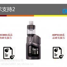
| Ʒ�ƣ�ŷ��о | �ͺţ�OC3001 | ���ͣ�����IC |
| ��;�������� | ���ʣ�12V | ���ţ�2018+ |
| ��ɫ����ԭ�����ṩ����֧�� | ����оƬ���ͣ�DC-DC | �������8 |
| ��װ��SOP8/DFN8 | ϵ�У�DC-DC | ��Ʒ˵����ԭװ��һ��ʮ |
| ��װ����� | Ӧ���������ܼҾ� |
OC3001
Dual Bootstrapped 12V MOSFET DRIVER
1 of 10
OC3001_V1.0
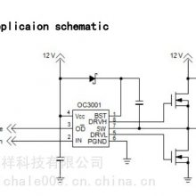
Typical applicaion schematic
General Descirption
The OC3001 is a single Phase 12V
MOSFET gate drivers optimized to drive the
gates of both highside and lowside power
MOSFETs in a synchronous buck converter.
The highside and lowside driver is capable
of driving a 3nF load with a 25ns propagation
delay and a 30ns transition time.
With a wide operating voltage range, high
or low side MOSFET gate drive voltage can
be optimized for the best efficiency. The
internal adaptive non-overlap circuit further
reduces the switching losses by preventing
simultaneous conduction of both MOSFETs.
The floating top driver design can
accommodate BST voltages as high as 40V,
with transient voltages as high as 48V. Both
gate outputs can be driven low by applying a
low logic level to the OD pin. An UVLO
function ensures that both driver outputs are
low when the supply voltage is low, and a
Thermal Shutdown function provides the IC
with over-temperature protection.
OC3001 is available in SOP8 and DFN8
package.
Features
AllInOne Synchronous Buck Driver
Bootstrapped HighSide Drive
One PWM Signal Generates Both Drives
Anti-cross Conduction Protection Circuit
These are PbFree Devices
Applications
Multiphase Desktop CPU Supplies
SingleSupply Synchronous Buck
Converters
e-cigarette
wireless chargerOC3001
Dual Bootstrapped 12V MOSFET DRIVER
2 of 10
OC3001_V1.0
Package and pin configuration
ODOD
Pin functions
pin Pin name Description
1 BST
Upper MOSFET Floating Bootstrap Supply. A
capacitor connected between BST and SWN pins
holds this bootstrap voltage for the highside
MOSFET as it is switched. The recommended
capacitor value is between 100nF and 1.0F. An
external diode is required with the OC3001
2 IN LogicLevel Input. This pin has primary control
of the drive outputs
3OD
Output Disable. When low, normal operation is
disabled forcing DRVH and DRVL low
4 VCCInput Supply. A 1.0 F ceramic capacitor should
be connected from this pin to PGND
5 DRVL Output drive for the lower MOSFET
6 PGND Power Ground. Should be closely connected to
the source of the lower MOSFET
7 SWN Switch Node. Connect to the source of the upper
MOSFET
8 DRVH Output drive for the upper MOSFETOC3001
Dual Bootstrapped 12V MOSFET DRIVER
3 of 10
OC3001_V1.0
Absolute maximum rating
symbol description value unit
VCCMaximum voltage on VDD pin 18 V
VMAX
Voltage range of BST/DRVH -0.3~48
V
Voltage range of DRVL -0.3~VCC+0.3
Voltage range of SWN -5~48
Voltage range of IN/OD-0.3~6.5
RJA
SOP8 thermal Resistance,
Junction-to-Ambient 123
o
C /W
DFN8 thermal Resistance,
Junction-to-Ambient 55
TAOperation temperature range -20~85
o
C
TSTGStorage temperature range -40~150
o
C
TSDWelding temp(less than 10sec.) 260
o
C
VESDESD(HBM) 2000 V
Functional block diagram
Figure1. Block DiagramOC3001
Dual Bootstrapped 12V MOSFET DRIVER
4 of 10
OC3001_V1.0
Electrical characteristics(VCC=12V,TA=0
o
C to 85
o
C, unless otherwise indicated)
Parameter Symbol Test Condition Min Typ. Max unit
Supply
Supply Voltage
Range
VCC- 4.6 13.2 V
Supply Current ISYSBST=12V, IN=0V 0.7 5 mA
ODInput
Input Voltage HighVOD_HI2 V
Input Voltage LowVOD_LO0.8 V
Hysteresis 400 mV
Input Current No internal pull-up or
pull-down resistors
-1 1 μA
PWM Input
Input Voltage High VPWM_HI2 V
Input Voltage Low VPWM_LO0.8 V
Hysteresis 400 mV
Input Current No internal pull-up or
pull-down resistors
-1 1 μA
High-Side Driver
Output Resistance,
Sourcing Current
BST-SWN=12V 2.2 3.4 Ω
Output Resistance,
Sinking Current
BST-SWN=12V 1.0 1.8 Ω
Output Resistance,
Unbiased
BST-SWN=0V 15 kΩ
Transition Times trDRVH
tfDRVH
BST-SWN=12V,
CLOAD=3.0nF
(See Figure 3)
20
18
55
45
ns
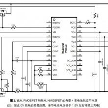
Propagation Delay
Times
tpdhDRVHBST-SWN=12V,
CLOAD=3.0nF
64 100 nsOC3001
Dual Bootstrapped 12V MOSFET DRIVER
5 of 10
OC3001_V1.0
tpdlDRVH
tpdlOD
tpdhOD
(See Figure 3)
(See Figure 2)
(See Figure 2)
15
5
18
30
15
35
SWN Pull-down
Resistance
SWN to PGND 15 kΩ
Low-Side Driver
Output Resistance,
Sourcing Current
1.8 3.4 Ω
Output Resistance,
Sinking Current
1.0 1.8 Ω
Output Resistance,
Unbiased
VCC=PGND 15 kΩ
Transition Times trDRVL
tfDRVL
CLOAD=3.0nF,
(See Figure 3)
18
15
50
30
ns
Propagation Delay
Times
tpdhDRVL
tpdlDRVL
tpdlOD
tpdhOD
CLOAD=3.0nF,
(See Figure 3)
(See Figure 2)
(See Figure 2)
59
10
10
20
100
30
35
35
ns
Timeout Delay BST-SWN=0V 85 ns
Under voltage Lockout
UVLO Startup 4.0 4.4 4.8 V
UVLO Shutdown 3.7 4.1 4.3 V
Hysteresis 0.1 0.3 0.5 VOC3001
Dual Bootstrapped 12V MOSFET DRIVER
6 of 10
OC3001_V1.0OC3001
Dual Bootstrapped 12V MOSFET DRIVER
7 of 10
OC3001_V1.0
Detail Description
Overview
The OC3001 are single phase MOSFET drivers designed for driving two Nchannel MOSFETs in a
synchronous buck converter topology. The OC3001 will operate from 5.0V or 12V, but have been
optimized for high current multiphase buck regulators that convert 12V rail directly to the core voltage
required by complex logic chips. A single PWM input signal is all that is required to properly drive the
highside and the lowside MOSFETs. Each driver is capable of driving a 3nF load at frequencies up to
1MHz.
Low-Side Driver
The lowside driver is designed to drive a groundreferenced low RDS(on)NChannel MOSFET. The
voltage rail for the lowside driver is internally connected to the VCCsupply and PGND.
High-Side Driver
The highside driver is designed to drive a floating low RDS(on)Nchannel MOSFET. The gate
voltage for the high side driver is developed by a bootstrap circuit referenced to Switch Node (SWN)
pin.
The bootstrap circuit is comprised of an external diode, and an external bootstrap capacitor. When
the OC3001 are starting up, the SWN pin is at ground, so the bootstrap capacitor will charge up to VCC
through the bootstrap diode. When the PWM input goes high, the highside driver will begin to turn on
the highside MOSFET using the stored charge of the bootstrap capacitor. As the highside MOSFET
turns on, the SWN pin will rise. When the highside MOSFET is fully on, the switch node will be at
12V, and the BST pin will be at 12V plus the charge of the bootstrap capacitor (approaching 24 V).
The bootstrap capacitor is recharged when the switch node goes low during the next cycle.
Safety Timer and Overlap Protection Circuit
It is very important that MOSFETs in a synchronous buck regulator do not both conduct at the same
time. Excessive shootthrough or cross conduction can damage the MOSFETs, and even a small amount
of cross conduction will cause a decrease in the power conversion efficiency.
The C3001 prevent cross conduction by monitoring the status of the external MOSFETs and
applying the appropriate amount of “deadtime” or the time between the turn off of one MOSFET and
the turn on of the other MOSFET.
When the PWM input pin goes high, DRVL will go low after a propagation delay (tpdlDRVL). The
time it takes for the lowside MOSFET to turn off (tfDRVL) is dependent on the total charge on the
lowside MOSFET gate. The OC3001 monitor the gate voltage of both MOSFETs and the switch node
voltage to determine the conduction status of the MOSFETs. Once the lowside MOSFET is turned off
an internal timer will delay (tpdhDRVH) the turn on of the highside MOSFET.
Likewise, when the PWM input pin goes low, DRVH will go low after the propagation delay
(tpdDRVH). The time to turn off the highside MOSFET (tfDRVH) is dependent on the total gate charge of
the highside MOSFET. A timer will be triggered once the highside MOSFET has stopped conducting,
to delay (tpdhDRVL) the turn on of the lowside MOSFETOC3001
Dual Bootstrapped 12V MOSFET DRIVER
8 of 10
OC3001_V1.0
Power Supply Decoupling
The OC3001 can source and sink relatively large currents to the gate pins of the external
MOSFETs. In order to maintain a constant and stable supply voltage (VCC) a low ESR capacitor
should be placed near the power and ground pins. A 1F to 4.7F multi layer ceramic capacitor
(MLCC) is usually sufficient.
Input Pins
The PWM input and the Output Disable pins of the OC3001 have internal protection for Electro
Static Discharge (ESD), but in normal operation they present relatively high input impedance. If the
PWM controller does not have internal pull-down resistors, they should be added externally to
ensure that the driver outputs do not go high before the controller has reached its under voltage
lockout threshold.
Bootstrap Circuit
The bootstrap circuit uses a charge storage capacitor (CBST) and the internal (or an external) diode.
Selection of these components can be done after the highside MOSFET has been chosen. The
bootstrap capacitor must have a voltage rating that is able to withstand twice the maximum supply
voltage. A minimum 50V rating is recommended. The capacitance is determined using the following
equation:
GATE
BST
BST
Q C =
V
Where QGATEis the total gate charge of the highside MOSFET, and VBSTis the voltage droop
allowed on the highside MOSFET drive. For example, a NTD60N03 has a total gate charge of
about 30nC. For an allowed droop of 300mV, the required bootstrap capacitance is 100nF. A good
quality ceramic capacitor should be used.
The bootstrap diode must be rated to withstand the maximum supply voltage plus any peak
ringing voltages that may be present on SWN. The average forward current can be estimated by:
F(AVG) GATE MAXI = Q f
where fMAXis the maximum switching frequency of the controller. The peak surge current rating
should be checked incircuit, since this is dependent on the source impedance of the 12V supply and
the ESR of CBST.OC3001
Dual Bootstrapped 12V MOSFET DRIVER
9 of 10
OC3001_V1.0
Package Information
SOP8 package outline dimensions:OC3001
Dual Bootstrapped 12V MOSFET DRIVER
10 of 10
OC3001_V1.0