�� ��
������
��0.01
200000 - 9999
��0.02
10000 - 99
��0.03
�۸�Ϊ�̼��ṩ�IJο��ۣ���ͨ��"��ȡ��ͱ���"
������������������λ~
��100
| Ʒ�ƣ���о | �ͺţ�WP820*** | ��װ��SOT23-6 |
| ���ţ��� | FET���ͣ����������� | ©Դ��ѹ(Vdss)������������ |
| ©������(Id)������������ | ©Դ��ͨ����(RDSOn)������������ | դԴ��ѹ(Vgs)������������ |
| դ�����(Qg)������������ | ����ָ�ʱ�䣺���������� | ����ɢ���ʣ�����������mW |
| �������ͣ����������� | �����¶ȷ�Χ������������ | ��װ���ͣ����������� |
WP820***
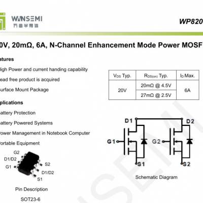
20V, 20mΩ, 6A, N-Channel Enhancement Mode Power MOSFET
1.Features
◆ High Power and current handing capability
◆ Lead free product is acquired
◆ Surface Mount Package
2.Applications
◆ Battery Protection
◆ Battery Powered Systems
◆ Power Management in Notebook Computer
◆ Portable Equipment
Pin Description
SOT23-6
VDS Typ.
RDS(on) Typ.
ID Max.
20V
20mΩ @ 4.5V
6A
27mΩ @ 2.5V
Schematic Diagram
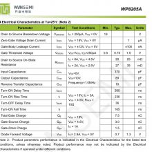
3.Absolute Max Ratings at Ta=25℃ (Note1)
Parameter
Symbol
Maximum
Units
Drain to Source Voltage
VDSS
19
V
Gate to Source Voltage
VGSS
±12
V
Drain Current-Continuous
ID
6
A
Drain Current (Pulse)
IDM
20
A
Maximum Power Dissipation
PD
1.9
W
Operating Junction and Storage Temperature Range
Tj,Tstg
-55 to +150
℃
Lead Temperature for Soldering Purposes
(1/8″ from case for 10 s)
TL
260
℃
Note 1: Stresses exceeding those listed in the Maximum Ratings table may damage the device. If any of
these limits are exceeded, device functionality should not be assumed, damage may occur and reliability may
be affected.
S1
D1/D2
S2
G1
D1/D2
G2
Rev.1.1 WAN SEMICONDUCTOR (NINGBO) CO.,LTD 2
WP820***
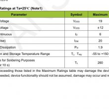
4.Electrical Characteristics at Ta=25℃ (Note 2)
Parameter
Symbol
Test Conditions
Min.
Typ.
Max.
Units
Drain to Source Breakdown Voltage
V(BR)DSS
ID = 250μA, VGS = 0V
19
V
Zero-Gate Voltage Drain Current
IDSS
VDS = 18V, VGS = 0V
1
μA
Gate-Body Leakage Current
IGSS
VGS = ±12V, VDS = 0V
±100
nA
Gate Threshold Voltage
VGS(th)
VDS=VGS, IDS=250μA
0.5
0.75
1.5
V
Drain to Source On-State
Resistance
RDS(on)
ID = 6A, VGS = 4.5V
20
25
mΩ
ID = 2A, VGS = 2.5V
27
35
mΩ
Input Capacitance
Ciss
VGS=0V,
VDS=10V,
Frequency=1.0MHz
370
pF
Output Capacitance
Coss
89
pF
Reverse Transfer Capacitance
Crss
10
pF
Turn-ON Delay Time
td(on)
VDD = 10V, ID = 3A,
VGS = 4.5V, RGEN =
10Ω
200
ns
Turn-ON Rise Time
tr
236
ns
Turn-OFF Delay Time
td(off)
36
ns
Turn-ON Fall Time
tf
165
ns
Total Gate Charge
Qg
VDS = 10V,
VGS = 4.5V,
ID = 1A
7.5
nC
Gate-Source Charge
Qgs
3.0
nC
Gate-Drain Charge
Qgd
1.5
nC
Diode Forward Voltage
VSD
IS = 2.8A, VGS = 0V
0.7
1.3
V
Note 2:Product parametric performance is indicated in the Electrical Characteristics for the listed test
conditions, unless otherwise noted. Product performance may not be indicated by the Electrical
Characteristics if operated under different conditions.
Rev.1.1 WAN SEMICONDUCTOR (NINGBO) CO.,LTD 3
WP820***
5.Typical electrical and thermal characteristics
Figure 1 Output Characteristics Figure 2 Transfer Characteristics
Figure 5 Rds(on) vs. Temperature Figure 6 Source to Drain vs. Temperature
Figure 3 Thershold Voltage vs. Temperature Figure 4 BVDSS vs. Temperature
Rev.1.1 WAN SEMICONDUCTOR (NINGBO) CO.,LTD 4
WP820***
Figure 11 Maximum Transient Thermal Impedence
Figure 9 Safe Operating Area Figure 10 Maximum Drain Current vs. Case Temperature
Figure 7 Capacitance Figure 8 Gate Charge
Rev.1.1 WAN SEMICONDUCTOR (NINGBO) CO.,LTD 5
WP820***
6.Package Dimensions
Rev.1.1 WAN SEMICONDUCTOR (NINGBO) CO.,LTD 6
WP820***
7.Important Notice
WAN SEMICONDUCTOR (NINGBO) CO.,LTD reserves the right to make corrections, enhancements,
improvements and other changes to its semiconductor products and services and to discontinue any product
or service. Buyers should obtain the latest relevant information before placing orders and should verify that
such information is current and complete. All semiconductor products (also referred to herein as
“components”) are sold subject to WANSEMI’s terms and conditions of sale supplied at the time of order
acknowledgment.
WANSEMI warrants performance of its components to the specifications applicable at the time of sale, in
accordance with the warranty in WANSEMI’s terms and conditions of sale of semiconductor products. Testing
and other quality control techniques are used to the extent WANSEMI deems necessary to support this
warranty. Except where mandated by applicable law, testing of all parameters of each component is not
necessarily performed.
WANSEMI assumes no liability for applications assistance or the design of Buyers’ products. Buyers are
responsible for their products and applications using WANSEMI components. To minimize the risks
associated with Buyers’ products and applications, Buyers should provide adequate design and operating
safeguards.
No WANSEMI components are authorized for use in FDA Class III (or similar life-critical medical
equipment) unless authorized officers of the parties have executed a special agreement specifically governing
such use.
Unless WANSEMI has specifically designated certain components which meet ***/TS16949
requirements, mainly for automotive use, WANSEMI will not be responsible for any failure of such
components to meet such requirements.